Parallel Port ATF and GAL Programmer
- Programs GAL16V8, ATF16V8B, GAL20V8, GAL22V10, ATF22V10B and ATF22V10C.
- Based on GALBlast by Manfred Winterhoff
- Plugs into PC Parallel Printer port.
- Works on Windows 3.1 and above (tested on an IBM Thinkpad 600 running Windows98)
I created this project because I wanted to program some GAL22V10 and
ATF22V10 PLDs which my so-called 'universal'
programmer wouldn't program properly. The hardware is a simplified
version of Manfred Winterhoff's GALblast.
I removed the parallel port buffers and replaced the DAC voltage
generator with a fixed +12V regulator. Programming voltage for GALs is connected
directly to the DC power jack and must be set manually, using a
suitable regulated power supply. I
modified the software so that it automatically switches the programming
voltage between +12V and Vin (14~16.5V) when writing to the GAL.
Update 2017-11-17: ATFBLAST V0.3 
After much research I finally figured how to properly program the
ATF22V10C!
Update 2017-11-22: ATFBlast V0.31
- fixed bug when writing UES to ATF22V10B
So far I have successfully programmed the following GALs/SPLDs:-
National GAL16V8
Lattice GAL16V8A, GAL16V8B, GAL16V8D
Lattice GAL22V10B
Atmel ATF16V8BQL, ATF22V10B, ATF22V10CQZ
More will be added to the list when I get samples to test.
Files for download
atfblast31.zip Executable for Windows 3.1/95/Xp, source code (compiles with Borland Turbo C++ V4.5)
ATFblast_v21 eagle.zip schematics and PCB layout in Eagle CAD format
conditio.jed JEDEC file for conditioning Atmel SPLDs
UPDATE 2018-05-7 PCB V2.1 corrected SELECT wiring, added resistors R6 and R7.
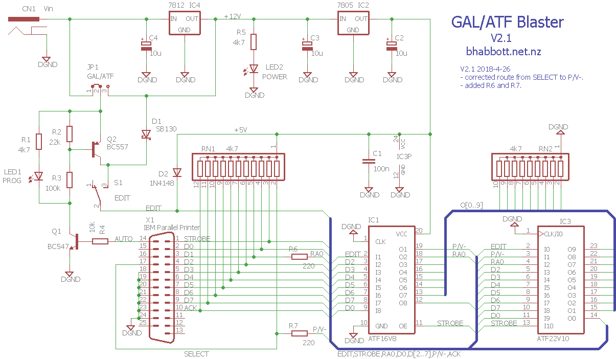
The circuit
Switch S1 puts the GAL into EDIT mode by applying +12V (via D1) to pin 2. Q1 and Q2 switch in the
higher voltage required for programming GALs. Jumper J1 is set
according to which type of chip (GAL or ATF) is being
programmed.
Q1 and Q2 can be any general purpose transistors such as 2N3904
and 2N3905 or 2SC945 and 2SA1015.
I used resistor arrays for the pull-ups and pull-downs, but discrete
resistors will also
work. D1 should be a Schottky type
for low voltage drop. As the GAL may draw up to 120mA (typically
60~70mA), the 5V regulator should have a heat sink installed.
For GALs the power input must be set to the programming voltage
specified for the particular chip (14V, 14.5V, 15.75V or 16.5V). For ATFs
it just needs to be high enough to ensure that the 12V regulator has
sufficient headroom (>=14V).
The PCB has sockets for ATF/GAL16V8 and ATF/GAL22V10. GAL20V8 requires a socket adapter to remap the pins.
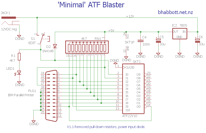
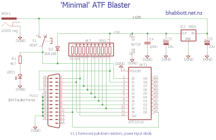
The 'Minimal' ATF Blaster is a further simplified circuit for
ATF chips. The 12V regulator and programming voltage control have
been removed, so the circuit must be powered from a well regulated +12VDC
supply. Since all ATF chips have pull-ups or pin keepers on their I/Os,
the pull-down resistors have also been removed. Pull-up resistors are
optional.They may be required if the printer port lines have low output voltage and/or high
capacitance.
Programming Procedure
1. Run ATFBLAST.exe, select LPT port and chip type.
2. Plug chip into programmer. Ensure that EDIT switch is turned OFF.
3. Plug programmer into LPT port.
4. Connect power to programmer.
5. Turn EDIT switch ON.
6. Click READ GAL to check that the chip is blank (all fuses = '1'). If not then you may need to erase it.
7. Load JEDEC file.
8. Click Write GAL. Check that detected chip matches the type selected.
9. Adjust power supply to the programming voltage shown in the dialog. *
10. Click Write PLD. (the 'PROG' LED will light for a second or two while programming)
11. Click Verify GAL. If verify fails then repeat steps 6-10.
10. Turn EDIT switch OFF.
11. Disconnect power from programmer.
12. Unplug programmer from LPT port.
13. Remove the programmed chip.
* Minimum input voltage on the 'Intelligent' programmer is 14V. When
programming ATF chips the jumper must be set to ATF mode.
If you just want to read PES information (programming voltage, pulse
durations, manufacturer etc.) you can click Write or Erase, then
Cancel.
Notes:
Conditioning
Atmel recommends that new SPLDs be 'conditioned' before programming.
This means that the whole device should be programmed with
0's twice and then erased. Verify errors can be ignored during conditioning. The blank JEDEC file conditio.jed is supplied for this purpose.
Write PES, Security, Erase All
These functions are provided for experimental purposes only and have not been tested. Use at your own risk!
Pull-up/down resistors, are they necessary?
To stop unused inputs from 'floating' and causing excessive
current draw, some GALs have internal pull-up resistors or
'pin-keepers' that hold the last input value.However most GAL16V8 and
GAL16V8B varieties do not have pull-ups, so all unused inputs
(including I/O pins programmed as inputs) need an external pull-up or
pull-down. Inputs left floating may change state during operation and
cause programming
errors.
Pull-ups are not strictly required on pins controlled by the
programmer, however they may improve signal rise time when using a
parallel port which has TTL outputs and/or high capacitance.
Why is GALblast not able to program Atmel SPLDs?
Manufacturers don't publish their programming algorithms (perhaps
because they are afraid of people making unreliable programmers that
could
damage their reputation) so DIYers have had to reverse engineer them.
This has
resulted in some misunderstandings and bad algorithms that may 'work'
for some chips but not others. Luckily I have a Stager VS4800 which
seems to program ATF chips correctly, so I monitored its operation with
a logic analyzer. Here is what I found:-
ATF PES is a text string
Unlike
normal GALs, the PES (Programmer Electronic Signature) in ATF
chips does not contain configuration information. Instead it has a
text string (stored byte reversed) representing the part number,
eg. "1F16V8B1" is an ATF16V8B. GALblast interprets this as
configuration information, which causes it to select the wrong programming
algorithm for the ATF16V8B.
P/V must be held low while sending bits to ATF22V10B/C
GALblast sets the P/-V (Program/Verify) pin high during the
entire time that the fuse and address bits are being sent. The correct
procedure is to keep P/V low while sending the bits, then pull it high
just before pulsing /STB to write the data.
Row address only requires 5 clocks on ATF22V10C
The ATF22V10C swaps the bit order of the row address and
changes the way that the bits are clocked into the chip. Only the first
5 bits are clocked in, then the last bit is sent without a
clock pulse. But GALblast clocks in all 6 bits, which divides the row addresses by 2.
UES is in a different location in ATF22V10
In ATF22V10 the UES (User Electronic Signature) is in the last 64
bits of row 44. This is the opposite of GAL22V10, where the UES is
in the first 64 bits.
ATF22V10CZ has Power Down function
By default the ATF22V10CZ uses pin 4 as a
'power-down' input. This feature needs to be turned off if pin 4 is
to be used as a logic input, otherwise pin 4 must be pulled low to enable
the chip. Disabling power-down is achieved by writing to row 59.